Learning KiCad
Learning KiCad has been interesting. Some things have been easy to learn after running through the tutorial. Others have taken some searching. Finding the right component is hard (like finding vertical electrolytic capacitors); the libraries are inconsistent and hard to browse. Figuring out how to place mechanical holes (NPTH—non-plated through hole) for “panelized” boards that snap apart took several google searches, and that was after I found a python script to run to panelize a design. The graphics handling is so 1980s, in that it draws garbage and expects you to regularly manually refresh to get rid of visual garbage on the display.
It probably would have been easier if I knew anything about PCB design when I started learning. Not knowing the techniques, the jargon, or the competing tools—and knowing next to nothing about electronic circuit design in general—makes simple things hard.
I’m guessing this is what it’s like for someone whose computer experience has been only superficial GUI use to suddenly drop down to the command line on Linux. ☺
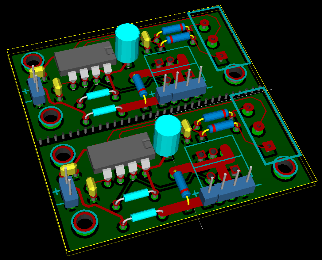
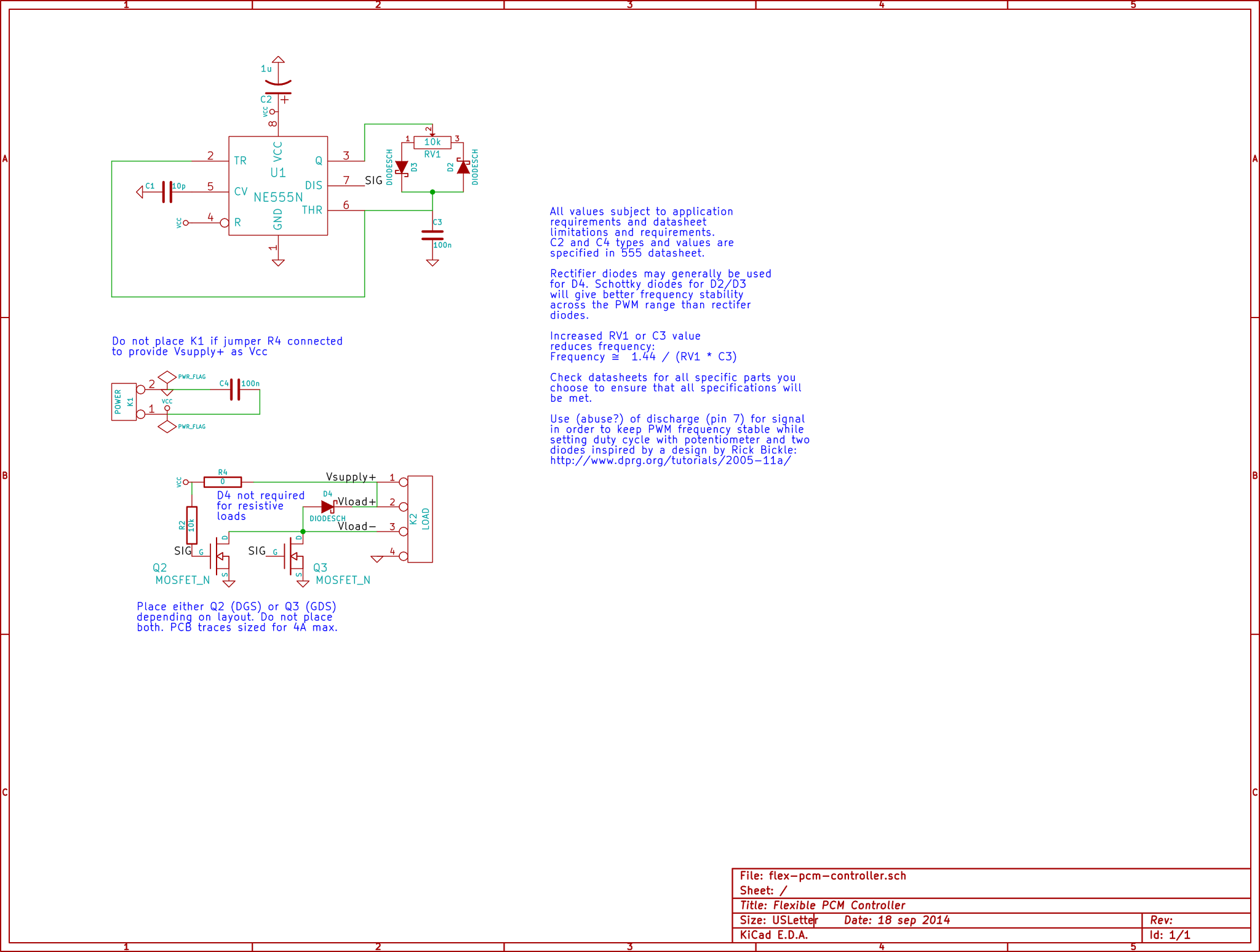
But I’m getting to the point that I can review git diff output of the output files to write useful changelog entries for myself; occasionally, hand-editing the textual data files (yay!) is easier than bringing up the GUI; and I’m approaching sending off my first order to dirtypcbs.com for my simple 555-based PWM controller.
Michael K Johnson September 18, 2014 22:45
I’m not using attiny for this for two reasons. One of my use cases is strings of LEDs, and the PWM frequency on attiny is too low—the flicker annoys me even with the attiny running at 8MHz where I did use attiny to provide PWM control for LEDs. Also, the 555 can run over a much wider voltage range, and the LED strings run at 12V, which is in spec for the 555 but would let the magic smoke out of an attiny. Otherwise attiny would be more flexible than a 555.
It was clear from very early in my experimentation that despite the KiCad oddities I have mentioned, Fritzing was a toy and KiCad was not, even though KiCad has plenty of rough edges.
The new (to me) european (?) resistor symbology felt weird at first but now I like it because I can put the value of the resistor in the box.
My seven year old son has volunteered to solder one of these, but I’m not sure he quite grasps how small a 2.5 x 5 cm board is. He’ll be able to stuff one of these with a small-signal BS170 MOSFET and use it to control a motor he pulled out of a dead CDROM drive, but I’m not sure yet what the motor is going to do when he’s done that. ☺
Michael K Johnson September 27, 2014 15:23
I found out that while I can panelize I can’t use NPTH for a snap line, so I will have to cut them instead. Also I choose the wrong time to try to order, right before Chinese national holiday! Oh, well. In the mean time I have learned that I should scan my design for acute angles that could be acid traps…
Michael K Johnson September 27, 2014 22:13
…and found one acid trap. Not bad since I didn’t know to avoid them before. ☺ I think credit goes to kicad because I think it doesn’t tend to create them when routing.
Since this is my first try, I wasn’t sure how much faith to put in the kicad 3D view. So last night I took a printout of the board at 100%, put stiff tape on the back, poked holes with a thumbtack, and stuffed the “board” with real components to make sure everything will actually fit. It was a pretty good match, and the biggest mismatch was that the 1uF electrolytic capacitor is smaller in real life than the 3D model I chose, which errs on the safe side.
Imported from Google+ — content and formatting may not be reliable